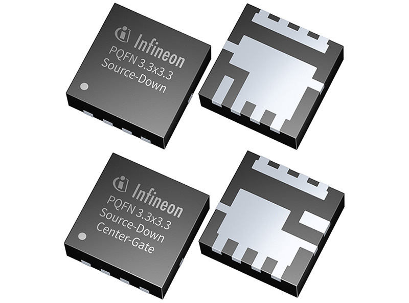
High power density, optimized performance, and ease of use are key requirements when designing modern power systems. To offer practical solutions for design challenges in end applications, Infineon Technologies AG (FSE: IFX / OTCQX: IFNNY) launches the new generation of OptiMOS™ Source-Down (SD) power MOSFETs. They come in a PQFN 3.3 x 3.3 mm 2 package and a wide voltage class ranging from 25 V up to 100 V. This package sets a new standard in power MOSFET performance, offering higher efficiency, higher power density, superior thermal management and low bill-of-material (BOM). The PQFN addresses applications including motor drives, SMPS for server and telecom and OR-ing, as well as battery management systems.
Compared to the standard Drain-Down concept, the latest Source-Down package technology enables a larger silicon die in the same package outline. In addition, the losses contributed by the package, limiting the overall performance of the device, can be reduced. This enables a reduction in RDS(on) by up to 30 percent compared to the state of the art Drain-Down package. The benefit at the system level is a shrink in the form factor with the possibility to move from a SuperSO8 5 x 6 mm 2 footprint to a PQFN 3.3 x 3.3 mm 2 package with a space reduction of about 65 percent. This allows for the available space to be used more effectively, enhancing the power density and system efficiency in the end system.
Additionally, in the Source-Down concept, the heat is dissipated directly into the PCB through a thermal pad instead of over the bond wire or the copper clip. This improves the thermal resistance R thJC by more than 20 percent, from 1.8 K/W down to 1.4 K/W, thus enabling simplified thermal management. Infineon offers two different footprint versions and layout options: the SD Standard-Gate and the SD Center-Gate. The Standard-Gate layout simplifies the drop-in replacement of Drain-Down packages, while the Center-Gate layout enables optimized and easier parallelization. These two options can bring optimal device arrangement in the PCB, optimized PCB parasitics, and ease of use.
OptiMOS™ Source-Down power MOSFETs are now available in PQFN 3.3 x 3.3 mm 2 packaging, a wide range of voltage classes from 25 up to 100 V, and two different footprint versions. More information is available at www.infineon.com/source-down.


![[전문가기고] K-배터리 3사, ‘Beyond EV’ 시장을 향한 기술 초격차 전략 비교 [인터배터리 2026] [전문가기고] K-배터리 3사, ‘Beyond EV’ 시장을 향한 기술 초격차 전략 비교 [인터배터리 2026]](https://icnweb.kr/wp-content/uploads/2026/03/battery-P3-beyond-Battery-web-1024x576.png)
![[심층기획] 피지컬 AI의 심장 ‘이차전지’, 휴머노이드 로봇 혁명 이끈다 [인터배터리 2026] [심층기획] 피지컬 AI의 심장 ‘이차전지’, 휴머노이드 로봇 혁명 이끈다 [인터배터리 2026]](https://icnweb.kr/wp-content/uploads/2026/03/Battery-pack-interB-Phy-AI.png)
![[데스크칼럼] 삼성 2030 AI 자율 공장 로드맵: 자동화를 넘어 ‘자율 제조’의 시대로 [데스크칼럼] 삼성 2030 AI 자율 공장 로드맵: 자동화를 넘어 ‘자율 제조’의 시대로](https://icnweb.kr/wp-content/uploads/2026/03/Gemini_Generated_Image_2030-AI-factory-1024web.jpg)





![[칼럼] 제조업 생존 가르는 EU CRA와 피지컬 AI 보안 전략 [칼럼] 제조업 생존 가르는 EU CRA와 피지컬 AI 보안 전략](https://icnweb.kr/wp-content/uploads/2026/03/CRA-2026-notebookLM-20260326-1024web.png)

![한국요꼬가와전기, 인터배터리 2026서 ‘배터리 자율 제조’ 비전 제시 [인터배터리 2026] 한국요꼬가와전기, 인터배터리 2026서 ‘배터리 자율 제조’ 비전 제시 [인터배터리 2026]](https://icnweb.kr/wp-content/uploads/2026/03/20260311_1604006789830108724224474-1024x576.jpg)


![[그래프] 국회의원 선거 결과 정당별 의석수 (19대-22대) 대한민국 국회의원 선거 결과(정당별 의석 수)](https://icnweb.kr/wp-content/uploads/2025/04/main-image-vote-flo-web-2-324x160.jpg)

